The high speeds of DDR IO and the very short data windows of DDR data pose significant challenges. For UMC 28nm Process.

Ddr Memory Interface Basics 2017 07 05 Signal Integrity Journal
22 DDR Interface Design Considerations.

. The speeds at which the memory controller must reliably operate 200 MHz across FR-4 PCB traces make the PCB layout challenging. Ad Browse discover thousands of brands. As the bandwidth requirement increases Double Data Rate DDR interface is becoming very commonly used in many types of memories such as DDR IIIIII DRAM RLDRAM III QDR IIIII SRAM etc.
Cadence Design IP portfolio comprised of an interface Denali. 13 PCB Stack-up The minimum stack-up for routing the DDR interface is a six-layer stack up. It provides additional general guidance for successful routing of high-speed signals.
Benefits of Alteras High-Speed DDR2 SDRAM Memory Interface Solution May 2004 ver. As the name implies SSTL is. For High-Speed Memory Controller and PHY Interface AUSTIN Texas May 2 2018 The DDR PHY Interface DFI Group today released version 50 of the specification for interfaces between high-speed memory controllers and physical PHY interfaces to support the requirements of future mobile and server memory standards.
SSTL leverage s an active motherboard termination scheme and overcomes the signal integrity concerns with legacy LVTTL signaling. Free 2-Day Shipping Free Returns. DRAM interface has been greatly increased to reduce the performance gap between the DRAM and the Central Processing Unit CPU.
Denali High-Speed DDR PHY IP. Building reliable high-speed memory interfaces target FPGA IO structures as well as intellectual property IP used within design software to allow rapid configuration of memory interfaces. Bandwidth for device memory.
As the bandwidth requirement increases Double Data Rate DDR interface is becoming very commonly used in many types of memories such as DDR IIIIII DRAM RLDRAM III QDR IIIII SRAM etc. These techniques use IP to help gain an extra timing margin at high speed operation. Digi-Key is Your Authorized Texas Instruments Distributor for Over 20 years.
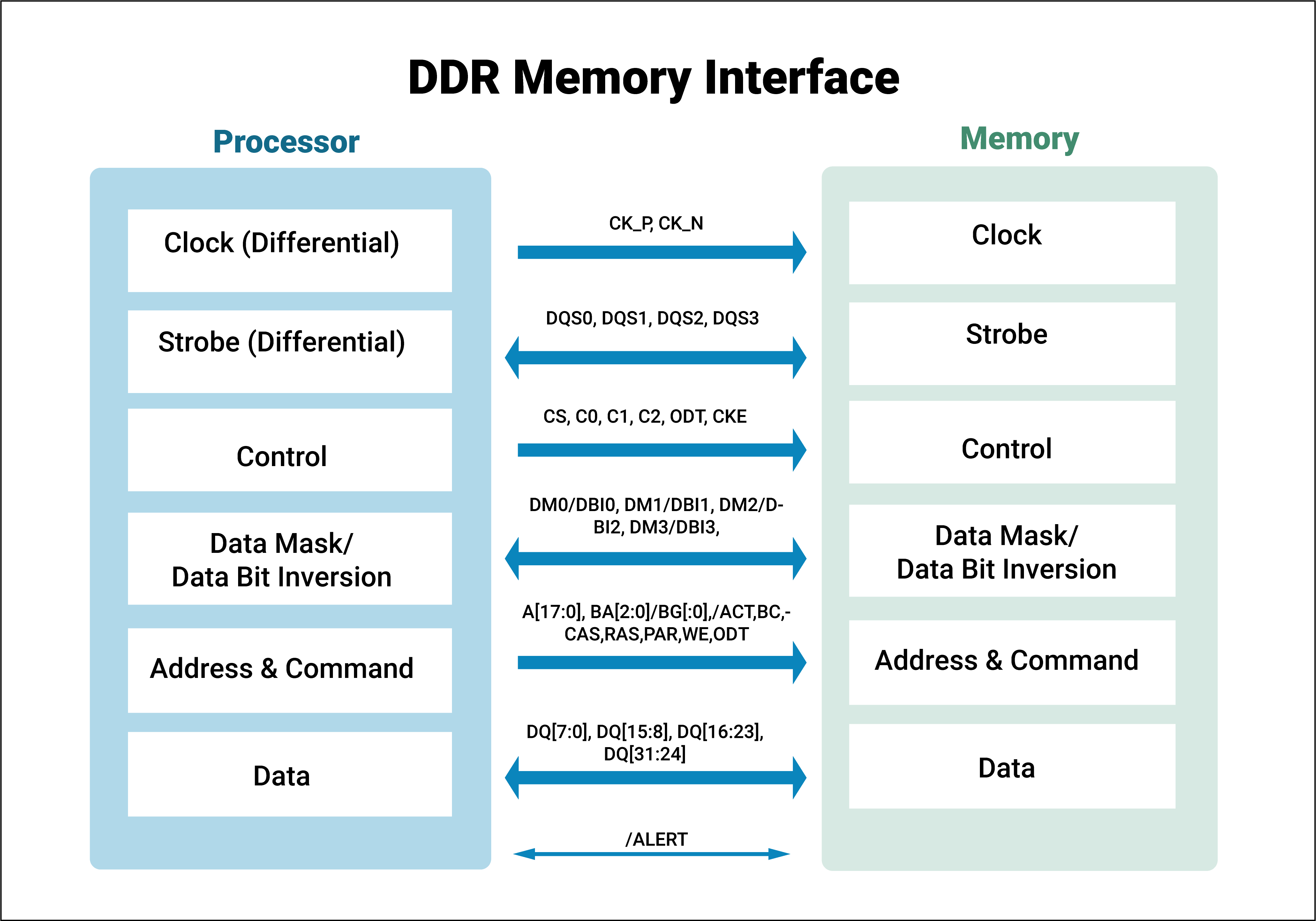
Memory interface analog and. Working closely with JEDEC Rohde Schwarz provides powerful solutions for DDR compliance testing. Winter 2016 ECE 153B - Sensor Peripheral Interface Design - The Memory Subsystem 26 DDR SDRAM Double Data Rate Synchronous Dynamic Random Access Memory Compared to single data rate SDR SDRAM the DDR SDRAM interface makes higher transfer rates possible by more strict control of the timing of the electrical data and clock signals.
However this can only be accomplished on a board with routing room with large keep-out areas. The Denali DDR PHY IP is part of the comprehensive. The major feature of DDR interface compared to a single data rate SDR one is to use both rising and falling edges of a clock to transfer data which allow it to provide two times the throughput at the same clock frequencyThe high speed up to 16 GHz for DDR III nature and complex timing issues take the most attention for designers of ASIC chips with DDR memory controllers.
High speed DDR memory interface design. The major feature of ddr interface compared to a single data rate sdr one is to use both rising and falling edges of a clock to transfer data which allow it. The Cadence Denali High-Speed DDR PHY IP provides low latency and 4266Mbps throughput while balancing power consumption and minimizing area.
09162014 AR58435 - Memory Interface UltraScale IP Release Notes 03312021 Supported Memory. The External Memory Interface EMIF Handbook is very. The need for increasing speed higher memory size and power efficiency is driving the evolution in DDR and LPDDR interface technology as defined by JEDEC.
The Altera External Memory Interface Handbook provides a thorough explanation of DDR4 topologies and board design guidelines for DDR4 systems. For DDR-I memories JEDEC created and adopted a low voltage high-speed signaling standard called series stub termination logic SSTL. DDR4 SDRAM operates at high data rate ie from 16Gbps to 32Gbps and the memory interface must be designed in a stringent way to comply with the specification set by JEDEC.
Ad Texas Instrument Boards Transistors ICs Power Supplies and More in Stock at Digi-Key. The CadenceDenaliDDR family of high-speed interface IP connects to external memories with the necessary bandwidth for applications. The data rate of double-data- rate DDR Synchronous DRAM SDRAM.
The DDR SDRAM uses DDR architecture to achieve high-speed operation. Nodes the Denali DDR PHY IP is designed to be robust under. Refer to the High-Speed Interface Layout Guidelines Application Report.
Varying noise conditions and to have interoperability with. Summary form only given. DDR SDRAM Main Controller Block Before it is operational the DDR SDRAM memory.
Introduction Date XTP359 - Memory Interface UltraScale Design Checklist PG150 - UltraScale Architecture FPGAs Memory IP Product Guide 08112021 PG150 - Creating a Memory Interface Design using Vivado MIG 08112021 Designing with UltraScale Memory IP. The Denali High-Speed DDR PHY IP provides low latency and up to 4266Mbps throughput while balancing power consumption and minimizing area Developed by experienced teams with industry-leading. Various supplier memory chips.
As part of the overall design DDR memory controller and memory. Ad Our Research Has Helped Over 200 Million People To Find The Best Products. The major feature of DDR interface compared to a single data rate SDR one is to use both rising and falling edges of a clock to transfer data which allow it to provide two times the.
View the Top 5 RAM of 2022. 10 1 WP-DDRIIFPGA-10 Introduction This white paper provides a general overview of the Double Data Rate 2 DDR2 SDRAM interface discusses some of the design challenges in DDR2 SDRAM and details Alteras solution used to implement. If you have significant high-speed signal runs on the microstrip layer then be sure to have accurate data.
DDR Memory Interface Design Considerations September 30 2011 2011 Micron Technology Inc. Design verification and debugging - Compliance testing. Furthermore incorporating the DDR interface into a flexible FPGA.
The DDRAM is based on 2n pre-fetch architecture that can achieve two data words per clock pulse at the IO pins for a single read or write access. External double data rate DDR memory types are a common part of many FPGA designs. Read customer reviews find best sellers.
Commandsclock topology for high-speed operation in a high-loading condition September 30 2011 2011 Micron Technology Inc. The Cadence Denali DDR family of high-speed interface IP connects to external memories with the necessary bandwidth for applications. The major feature of DDR interface compared to a single data rate SDR one is to.
All the major challenges discussed in this paper have to be overcome for excellent signal integrity to guarantee minimum bit error rate in the multi-Gigabit transmission.
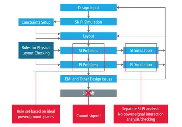
Implement Si And Pi In High Speed Memory Interfaces Signal And Power Integrity Pcb Ic Packaging Cadence Blogs Cadence Community
2

Ddr Phy Ip For Soc Designs Cadence Ip
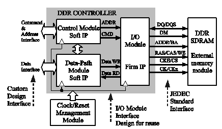
Ddr Sdram Controller Ip Designed For Reuse
Ddr Memory And The Challenges In Pcb Design Sierra Circuits

How To Successfully Realize A High Speed Memory Interface In Your Design
Figure 1 From Design And Implementation Of High Speed Ddr Sdram Controller On Fpga Semantic Scholar

Pdf High Bandwidth Memory Interface Design Based On Ddr3 Sdram And Fpga Semantic Scholar
0 comments
Post a Comment